


In next-generation semiconductor manufacturing and high-density PCBA production, semiconductor inspection accuracy directly impacts yield, reliability, and production efficiency.
As chip architectures become smaller, thinner, and more complex, traditional visible light inspection systems face fundamental limitations. Visible cameras can only capture surface information because silicon wafers behave like optical mirrors, preventing engineers from seeing hidden structures beneath the surface.
To overcome these challenges, manufacturers are adopting SWIR imaging technology and InGaAs infrared cameras to enable non-destructive wafer inspection, internal defect detection, and advanced semiconductor failure analysis.
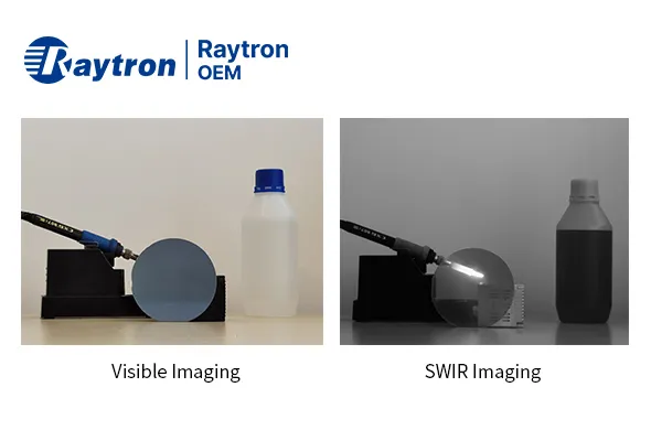
Why Silicon Becomes Transparent Under SWIR
SWIR Enables See-Through Silicon Inspection.
Traditional optical inspection using visible wavelengths cannot penetrate silicon due to its crystalline structure and optical absorption characteristics.
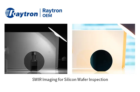
However, SWIR wavelengths (900 nm–1700 nm) interact differently with silicon materials. At specific infrared wavelengths, silicon becomes highly transparent, allowing infrared radiation to pass through the substrate.
Powered by advanced InGaAs sensors, SWIR cameras can capture hidden structures inside semiconductor devices that are invisible to conventional cameras.
This breakthrough enables:
- Advanced wafer-level packaging analysis
- Non-destructive silicon wafer inspection
- Internal semiconductor defect detection
- Subsurface imaging of chip structures
Applications on the Production Line
Integrating SWIR imaging directly into high-throughput production lines solves several of the most complex challenges in modern electronics manufacturing:
- Real-Time Crack Analysis: Identify microscopic fractures caused by thermal or mechanical stress during high-speed dicing and packaging processes.
- Subsurface Defect Detection: Locate internal voids, micro-cracks, and impurities hidden deep within the silicon bulk before they lead to catastrophic component failure.
- Inner-Layer Alignment: Inspect and verify the precise alignment of multi-stacked dies and wafer-to-wafer bonding in 3D semiconductor architectures.
How Do SWIR Cameras Improve Semiconductor Inspection Through Compact OEM Integration
Upgrading an inspection line shouldn’t require rebuilding the entire factory layout. SWIR solutions feature strict SWaP-C optimization.
Our ultra-sensitive InGaAs technology is packed into miniature OEM cores. For example, NS-615A-GE area scan SWIR camera module integrates advanced InGaAs sensor technology into a compact industrial imaging platform, providing high-sensitivity SWIR imaging capabilities for semiconductor inspection, wafer analysis, and machine vision applications.
Designed for seamless OEM integration, the NS-615A-GE delivers the flexibility required by system developers to incorporate SWIR imaging into Automated Test Equipment, robotic inspection arms, and customized semiconductor inspection systems.
These compact modules integrate seamlessly into your existing production environments. They eliminate production bottlenecks, require no extra floor space, and protect your existing capital investments.By moving from visible light to SWIR solutions, manufacturers can drastically shorten failure analysis cycles, reduce scrap rates, and maximize overall manufacturing yield.
About Raytron OEM
Raytron OEM, a wholly-owned subsidiary of Raytron Technology Co., Ltd., is a leader in uncooled infrared thermal imaging. With full-stack capabilities from IC and MEMS sensor design to system integration, we deliver high-performance infrared solutions for industrial monitoring, wildfire prevention, outdoor night vision, consumer electronics, and intelligent sensing. Guided by our mission, “To Create Incremental Value for Customers with Technological Advancements”, we continue to drive innovation and empower smarter, safer, and more efficient systems worldwide. For more on the Raytron Microelectronics program, visit: https://www.raytron-microelectronics.com/contact-us