


ermines its size and how easily it integrates into a system. So how do you pack more components into limited space and shrink the footprint even further? On September 9, 2026, at the China International Optoelectronic Expo (CIOE), Raytron OEM, the detector and module brand of Raytron, unveiled the industry’s first new packaging solution: BCoS (Bump Chip on Substrate) packaging.
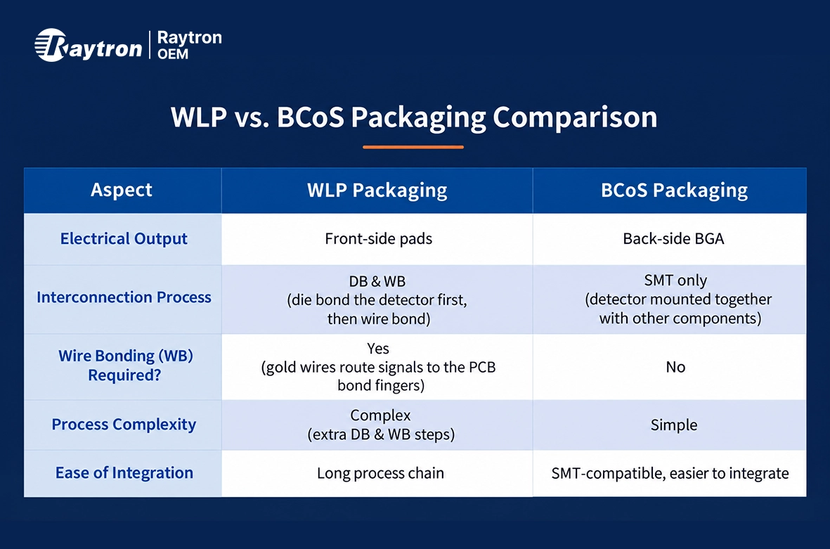
Built on advanced packaging technology, the BCoS detector uses Through Silicon Via (TSV), Redistribution Layer (RDL), and metal bump structures to route its electrical signals out through a ball grid array (BGA) on the back. To interconnect with an external PCB, it simply goes through surface-mount technology (SMT) with the other components to complete the printed circuit board assembly (PCBA). It eliminates the need for bond finger space on the PCB, as well as the die bonding (DB) and wire bonding (WB) steps. The result is a smaller module and a simpler process. BCoS detectors can now be delivered to customers in small batches.
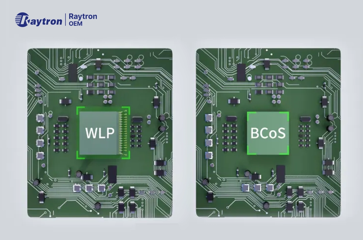
With conventional Wafer-Level Packaging (WLP) uncooled infrared detectors, mounting the detector and connecting it electrically to the PCB both require DB and WB. This complicates module assembly and calls for extra bond fingers on the PCB, which makes it hard to meet the demand for smaller modules.
The Significance of BCoS Packaging
A Thinner Chip for Slimmer Products and More Design Flexibility
The 256 × 192 @ 12 μm BCoS detector is only about 1.14 mm thick, roughly 21% thinner than a WLP detector of the same specification (1.455 mm). End products can be thinner and lighter, which gives them an edge in size-sensitive markets such as portable devices and consumer electronics.
A Smaller Module for Tighter Integration and More Applications
A BCoS detector connects to the PCB through vertical interconnection, so no bond fingers are needed. Compared with a conventional module, this cuts the detector’s footprint by nearly 40%. The chip itself is also thinner, so the module shrinks both laterally and vertically. A smaller module is easier to embed in space-constrained designs, opening up applications that range from industrial temperature measurement and security and firefighting to smart home and consumer devices.
One Fewer Process Step: Easier Integration and More Stable Yield
A WLP detector requires additional DB and WB steps, which lengthen the process chain. A BCoS detector goes through SMT together with the other components, completing mounting and electrical interconnection in a single step. One fewer process step means one fewer potential point of failure, which lowers the barrier to adoption and improves product yield.

As a leader in infrared thermal imaging, Raytron OEM has always stayed true to its purpose: To Create Incremental Value for Customers Through Technological Advancement. As infrared thermal imaging accelerates its move from industrial-grade to consumer-grade applications, size is becoming the industry’s first hurdle, and BCoS packaging is Raytron OEM’s answer.
BCoS packaging is more than a packaging innovation; it takes miniaturization to the extreme. By streamlining integration and development, it makes the key upstream component easier to design in, so the infrared core can reach more applications with a smaller footprint and a simpler process.
Every micron cut from the package size opens the door to another infrared application. That is the real significance of BCoS packaging: fitting professional-grade infrared capability into ever smaller spaces.